|
||||
| News and Information about the Test of Electronics in Research & Design, Production, Maintenance, and Installation. | ||||

Main MenuNewsletterNews AreaInfo AreaWeblinksProduct Focus |

Readers Top 5 News of last 30 days
Latest Test and Measurement NewsReview and Classification of Ultra-Small Photomask Defects
Like its predecessor, the E5620 implements Advantest’s highly stable image capture technology to easily import defect location data from mask inspection systems and automatically image the locations. The system has a number of improvements specifically to target future mask requirements. “In working with our customers to determine their requirements for the future EUV photomask inspection and analysis, we identified several essential advancements to integrate into our proven DR-SEM system,” said Toshimichi Iwai, senior VP of the Nanotechnology Business Group with Advantest. “With the E5620, our team of lithography experts has created a superior tool that can handle today’s photomasks and is truly future-ready for the coming EUV generation.” E5620 Key New Features
The E5620 DR-SEM is available for purchase now. www.advantest.com/ Related Articles: |

Upcoming Events More events...
Tag CloudOscilloscope
JTAG
Boundary Scan
Goepel
PXI
Rohde & Schwarz
Tektronix
Keysight
AOI
Anritsu
National Instruments
Inspection
Teledyne LeCroy
Aeroflex
LTE
Yokogawa
AXI
Spectrum Analyzer
Keithley
In-Circuit-Test
Signal Analyzer
Automotive
EMC-Test
Signal Generator
Advantest
Multitest
B&K Precision
Corelis
Power Supply
SPI
Flying Prober
Teseq
Cognex
Switching
Teradyne
Viscom
Pickering
Fluke
GAO Tek
PCIe
|
||
|
© All about Test 2018 |
||||
 How to resolve AdBlock issue?
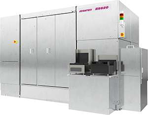 20 December 2022 – Advantest unveiled the E5620 Defect Review Scanning Electron Microscope (DR-SEM), its newest mask SEM product for reviewing and classifying ultra-small defects on photomasks and mask blanks. With its high-accuracy, high-throughput defect review capability, the E5620 DR-SEM is expected to contribute appreciably to production quality improvements in next-generation photomasks and shorter mask manufacturing turnaround times.