 |

Main Menu
Newsletter
News Area
Info Area
Weblinks
Product Focus

 How to resolve AdBlock issue?
 Readers Top 5 News of last 30 days
- 03 April 2024 - 5-in-1 Programmable Oscilloscopes
- 05 April 2024 - Oscilloscope Days event in April 2024
- 28 March 2024 - RF Test Enclosures provide highly-isolated Bench-top Environments
- 11 April 2024 - Flying Probe Tester for Probe Cards
- 02 April 2024 - Advantest appointed new Group CEO
News - Component Test
 Wafer Scanner Inspection System
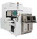
14 June 2011 — Rudolph Technologies, Inc. announced the availability of the new Wafer Scanner 3880 System. The WS 3880 provides 3D (height) and 2D measurement and inspection of micro and standard bumps, through silicon via (TSV) post-via-fill copper protrusions (nails) and re-distribution layers (RDL) used in 3D IC packaging.
It also offers an ultra-high resolution 3D sensor designed specifically for micro bumps as small as a few microns. The WS 3880 is ideal for high-volume manufacturing, combining performance and throughput for either randomly sampled inspection or 100 percent inspection.
According to Reza Asgari, Rudolph’s Wafer Scanner product manager, “Micro bumps, TSVs and RDLs are critical interconnect technologies used in 3D IC packages; the new WS 3880 provides the 2D and 3D measurement and inspection capability required to develop and maximize yields for these packaging processes. Ultra-high resolution allows the Wafer Scanner to accurately characterize small features, such as micro bumps and TSV nails, which manufacturers are using to achieve unprecedented connection densities between chips, while still preserving the flexibility to handle standard bumps and other larger features.”
Asgari added, “Flexibility, throughput and inspection performance were primary considerations for the first production system, delivered in March 2011 to a major semiconductor foundry. The ability to look at a range of bump and RDL sizes and types was critical for the second system that shipped to a leading IDM where it will be used to develop new packaging processes.”
The WS 3880 replaces the highly successful 3840 system, launched immediately following Rudolph’s acquisition of RVSI assets in 2008. Over 20 WS 3840 systems have been installed in advanced packaging facilities.
The WS 3880 is a comprehensive wafer inspection system, providing a fast, flexible and reliable inspection and metrology solution for bump, RDL and TSV nail processes in advanced semiconductor device packaging. It can inspect both flip chip and non-flip chip wafers. The base system provides high throughput, image-based macro defect inspection, as well as measurements of bump diameter and position, RDL width, and other 2D parameters. Rudolph’s proprietary 3D laser triangulation technology measures bump height and coplanarity, RDL thickness, and much more. The system permits on-line or off-line defect review and classification. Electronic wafer maps can be imported into the system, updated after inspection and exported.
The WS 3880 system is now commercially available and can be ordered immediately.
www.rudolphtech.comRelated Articles:

Upcoming Events
More events...
See our Trade Show Calendar
Click here
Tag Cloud
© All about Test 2018