 |

Main Menu
Newsletter
News Area
Info Area
Weblinks
Product Focus

 How to resolve AdBlock issue?
 Readers Top 5 News of last 30 days
- 11 April 2024 - Flying Probe Tester for Probe Cards
- 24 April 2024 - PC-based control makes quality audible
- 10 April 2024 - HiL Software for more Efficient Testing
- 09 April 2024 - Protocol Test Solution supporting NTN NB-IoT Devices for GEO Satellites
- 25 April 2024 - EMI-Analyzer for EMC Standards Measurements
News - General T&M
Hioki launched Flying Probe Tester for PCBs
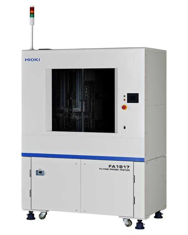 13 February 2019 - Hioki launched the Flying Probe Tester FA1817, an automatic testing system designed to inspect printed wiring on bare boards. The FA1817’s features and capabilities make it ideal for use in inspecting high-density printed wiring boards.
With support for a broad range of test types, from low-resistance measurement to high-insulation-resistance measurement, the system reliably detects the latent defects that trouble end-users.
In addition, Process Analyzer, a newly developed application that ships standard with the FA1817, makes it easy to create statistical data based on on test results and to analyze defects. In this way, the system can be used not only to perform pass/fail testing, but also as an aid in realizing process improvements.
Key Features
- Support for a broad range of test types, from low-resistance measurement to high-insulation-resistance measurement
Hioki has taken advantage of its exceptional technological capabilities in the areas of low-resistance measurement and insulation resistance measurement to deliver the ability to measure low resistance as well as high insulation resistance of 100 GΩ/250 V (when using dedicated probes and measurement boards).
The FA1817’s low-resistance measurement functionality measures minuscule fluctuations in resistance values to detect open-via defects. By means of its high-insulation-resistance measurement capabilities, the system also detects insulation abnormalities and arc discharge phenomena caused by the effects of pattern shape anomalies and impurities, voids, and other defects that exist between patterns.
- Half the impact depth
Traditionally, probes are placed in contact with the board to carry out bare board testing in a process that leaves impact marks on the board. On high-density bare boards, even small marks can have a serious effect. Impact marks from the probes of previous products were already slight, but the FA1817 uses the High-density Probe CP1072, which was developed using proprietary Hioki technology, in order to further reduce the size and depth of these marks. Impact mark depth has been halved compared to that of previous products to minimize damage to bare boards.
- Optimized probe movement for testing that’s up to 20% faster
By taking advantage of two top arms and two bottom arms to probe target boards efficiently, the FA1817 reduces testing times by up to 20%.
- Defect analysis with the newly developed Process Analyzer (a standard accessory)
The Process Analyzer application makes it easy to load accumulated test results data in a batch and then create statistical data from it. Test step results can be visualized using such means as value changes, histograms, and distribution maps to facilitate analysis of defects. By generating information about analyzed defects that can be provided as feedback to design and manufacturing processes, the Process Analyzer helps customers improve yields in printed wiring board manufacturing.
www.hioki.com/
Related Articles:

Upcoming Events
More events...
See our Trade Show Calendar
Click here
Tag Cloud
© All about Test 2018