|
||||
| News and Information about the Test of Electronics in Research & Design, Production, Maintenance, and Installation. | ||||

Main MenuNewsletterNews AreaInfo AreaWeblinksProduct Focus |

Readers Top 5 News of last 30 days
Latest Test and Measurement NewsSignal Integrity Simulation Software
After completing a PCB design, hardware engineers hand the design over to SI specialists to validate its performance before going to prototype. SI specialists perform simulations on a large number of nets, which can take days to weeks to complete. As a result, hardware engineers have difficulty predicting how much analysis time it will take to find errors or performance issues in the design. Uncertainty about the length of the SI analysis phase creates a bottleneck in the design cycle and delays time-to-market. EP-Scan addresses SI analysis bottlenecks by giving hardware designers diagnostic tools to correct designs earlier and meet development schedules. As a stand-alone software product, EP-Scan performs electromagnetic (EM) simulation on signal nets and reports SI metrics such as channel return and insertion loss. In addition, EP-Scan automates performance comparisons between different versions of a design and generates simulation reports that expedite verification prior to building expensive physical prototypes. "Our goal with EP-Scan is to 'shift left' the PCB design verification process by using early simulation to detect and correct errors, giving hardware designers the confidence to move forward and obtain first pass success," said Tim Wang-Lee, Ph.D., Product Marketing Manager at Keysight. "I am proud that EP-Scan is helping engineers to spend more time doing analyses to gain insights, documenting results to track progress, and automating routine tests. EP-Scan empowers hardware engineers by maximizing their productivity." EP-Scan requires only the layout geometry and substrate stack-up information for the PCB design as inputs. After engineers specify the desired nets for investigation, EP-Scan reports simulation results including the characteristic impedance and delay of traces, return loss, insertion loss, and impedance time-domain reflectometry (TDR). By analyzing common fabrication formats such as ODB++, EP-Scan shows engineers the performance of their design as it would be when fabricated. EP-Scan enables hardware engineers to quickly validate designs and identify layout issues before the final verification, which reduces time-to-market, and can contribute to more PCB design wins. www.keysight.com/ Related Articles: |

Upcoming Events More events...
Tag CloudOscilloscope
JTAG
Boundary Scan
Goepel
PXI
Rohde & Schwarz
Tektronix
Keysight
AOI
Anritsu
National Instruments
Inspection
Teledyne LeCroy
Aeroflex
LTE
Yokogawa
AXI
Spectrum Analyzer
Keithley
In-Circuit-Test
Signal Analyzer
Automotive
EMC-Test
Signal Generator
Advantest
Multitest
B&K Precision
Corelis
Power Supply
SPI
Flying Prober
Teseq
Cognex
Switching
Teradyne
Viscom
Pickering
Fluke
GAO Tek
PCIe
|
||
|
© All about Test 2018 |
||||
 How to resolve AdBlock issue?
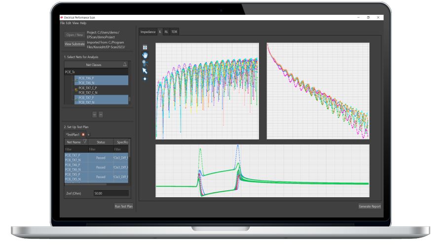 02 February 2023 - Keysight Technologies introduced the Electrical Performance Scan (EP-Scan), a new high-speed digital simulation tool that supports rapid signal integrity (SI) analysis for hardware engineers and printed circuit board (PCB) designers. EP-Scan provides electrical performance insights that enable high-speed digital designers to perform quick diagnostics and remove the verification bottleneck. It identifies layout issues quickly, catches design inconsistencies early, and creates design progress reports effortlessly.